
Prototyping and Fabrication Facility

The Rapid Prototyping Lab is a cutting-edge facility designed to empower researchers, students, and innovators with the tools to bring their ideas to life. Equipped with state-of-the-art technologies, the lab facilitates, the rapid creation, testing, and refinement of prototypes, bridging the gap between concept and reality (above image; Tile-scanned images of vasculature networks (green) and LS perfusion (red) alongside an overlayed image of both channels, taken using a confocal microscope (10× objective). LS were observed to enter the chamber from the high pressure side channel (right) and perfuse across the network. Right side images shows high magnification images (50× objective) showing LS perfusing exclusively through networks and remaining confined within the vessels. Images were taken from multiple chips - https://pubs.rsc.org/en/content/articlehtml/2023/lc/d2lc00963c).
The Lab features advanced 3D printing technologies, including high-resolution optical and resin-based printers, capable of producing intricate and precise models. .
The space fosters interdisciplinary collaboration across engineering, material science, design and manufacturing. Applications of the lab span various domains, including product development for innovative consumer goods, healthcare solutions such as custom medical devices, hands-on STEM education experiences for students, and research involving advanced technologies and experimental setups.
The Rapid Prototyping Lab is more than just a workspace; it’s a hub of creativity and exploration. By providing access to the latest tools and technologies, the lab empowers users to transform ideas into tangible results quickly and efficiently.

Fabrication Tools

Explore some of our cutting-edge instruments, designed to support advanced research and detailed analysis. Each instrument is selected to enhance hands-on-learning and innovative discovery.

Oxygen Plasma Surface Technology (Diener)

Oxygen Plasma Surface Technology (Diener)

Diener Plasma Surface Technology offers state-of-the-art solutions for surface treatment and modification through advanced plasma technology. This process is suitable for a wide variety of materials and applications, enhancing the performance, adhesion, and cleanliness of surfaces. By utilizing a low-temperature, highly energized state of matter, plasma, it effectively modifies both the chemical and physical properties of a material’s surface.
Plasma surface treatment involves exposing surfaces to reactive ions and radicals within the plasma, which allows for several beneficial modifications. These include cleaning surfaces at a molecular level, improving adhesion properties for coatings or bonding, and adjusting surface energy to make surfaces hydrophilic or hydrophobic. Additionally, it can etch or structure materials with high precision, making it a versatile tool in many industries.
One of the significant advantages of Diener Plasma Systems is their wide range of applications. These systems can treat various materials, including plastics, metals, ceramics, glass, and composite materials, making them adaptable to different industrial and research needs. The technology is also environmentally friendly, using minimal chemicals and energy, which reduces its environmental impact compared to traditional surface treatment methods.
The customizable nature of the plasma systems is another notable feature. Users can adjust process parameters, such as pressure, gas composition, and treatment time, providing precise control over the treatment process. This allows researchers and manufacturers to tailor the technology to specific materials and desired outcomes.
Diener Plasma systems are safe and efficient, utilizing non-toxic, gentle processes that ensure the integrity of even the most delicate substrates. This makes the technology particularly beneficial for industries where material preservation is critical, such as in the medical device and electronics sectors.
Key applications of Diener Plasma technology span a broad range of industries. In adhesion enhancement, plasma treatment improves the bonding of coatings, adhesives, and inks. It also plays a crucial role in surface cleaning, removing organic contaminants to ensure ultra-clean surfaces. For medical devices, it sterilizes and functionalizes surfaces to ensure biocompatibility. In electronics, it modifies surfaces to enhance soldering and coating adhesion. Finally, in industries such as aerospace and automotive, it optimizes adhesion for paints, composites, and seals.
Overall, Diener Plasma Surface Technology is a critical tool for industries and research facilities that require innovative, precise surface solutions. With its versatility, eco-friendly approach, and ability to meet the demands of modern manufacturing and material research, it continues to drive advancements in surface treatment and modification.

Saturn 4 Ultra 16K - High-Precision Resin 3D Printer (Elegoo)

Saturn 4 Ultra 16K - High-Precision Resin 3D Printer (Elegoo)

The Elegoo Saturn 4 Ultra 16K is a resin-based 3D printer available within the Rapid Prototyping lab. It utilizes a 10-inch monochrome LCD and an ultra-high 16K resolution panel, the printer achieves an outstanding level of precision, making it ideal for research laboratories, engineering workshops, product-development environments, and educational institutions requiring reliable and repeatable results.
With an extremely fine X-Y resolution of 14 x 19 μm and a display resolution of 15120 x 6230 pixels, the Saturn 4 ultra 16K brings even the finest details to life. With a generous build volume of 211.68 × 118.37 × 220 mm, the Saturn 4 Ultra 16K accommodates small, detailed components and medium-sized models, enabling a range of projects across different disciplines. The system offers high accuracy suitable for applications requiring fine geometries or smooth surface finishes. The uniform optical engine and 16K monochrome exposure screen contribute to consistent curing across the build plate, supporting the production of detailed features such as those found in micro-structured components, microfluidic device moulds, and precision laboratory fixtures. The Z-axis can operate with a layer thickness between 0.01 and 0.2 mm, with a positional accuracy of 20-micron (0.02 mm).
The printer operates using MSLA (Masked Stereolithography Apparatus) technology. It employs a COB (Chip-On-Board) LED array combined with a Fresnel Collimating Lens to deliver even UV light exposure at 405 nm. This configuration helps maintain dimensional accuracy and structural integrity across prints and reduces artefacts associated with uneven light distribution.
The printer incorporates an innovative tilt-release technology that reduces peeling forces during layer separation, supporting more stable printing and potentially reducing print failures. Under suitable conditions, the system can reach print speeds of up to 150 mm/h without compromising on quality. This dramatically shortens production time, enabling rapid prototyping, quick iteration cycles, and efficient small-batch manufacturing.
The machine also includes a Smart Resin Heating System (Smart Tank Heating), which maintains resin at approximately 300C. Consistent resin temperature helps secure stable viscosity, improved bonding between layers, and reproducible results – particularly useful in environments with fluctuating ambient temperatures.
The Elegoo Saturn 4 Ultra 16K is particularly well suited for environments where precision, speed, and reliability are essential. Its capabilities support a wide range of disciplines, prototyping of micro-mechanical components, fabrication moulds for microfluidic or analytical devices, or creating customised laboratory fixtures or adaptors when precision is required.
The Elegoo Saturn 4 Ultra 16K is a versatile, and highly precise resin 3D-printing system that bridges the gap between professional-grade manufacturing and accessible laboratory use. Its combination of ultra-fine resolution, fast production speeds, large build capacity, intelligent automation, and stable optical performance makes it an invaluable tool for researchers, engineers, designers, and students alike.
Whether used for precision prototyping, experimental research apparatus, or high-detail educational models, the Saturn 4 Ultra 16K offers exceptional performance and reliability—making it a robust and future-ready asset for any modern university laboratory or research facility.

P1S - 3D Printer (Bambu Lab)

P1S - 3D Printer (Bambu Lab)The Bambu Lab P1S is an advanced FDM (Fused Deposition Modelling) based additive manufacturing system designed for fast, accurate, and highly repeatable production of functional 3D-printed components. Engineered with a rigid Core XY motion (up to 20 m/s2 acceleration) architecture, an actively controlled enclosed chamber, all-metal hot end temperature (max 3000C), with nozzle diameter of 0.4 mm and 0.2 mm, having 500 mm/s maximum speed of toolhead and up to 16-colour printing with AMS (Automatic Material System), the P1S delivers exceptional speed, dimensional stability, and material versatility. This makes it particularly suitable for university research laboratories, engineering workshops, product-development environments, and teaching spaces requiring dependable day-to-day performance.
With a generous build volume of 256 × 256 × 256 mm3 (10 x 10 x 10 inches), the P1S offers the capacity to produce medium-sized prototypes, mechanical components, customised jigs and fixtures, and multiple smaller parts simultaneously. Paired with its high-speed motion system and advanced thermal control, the printer provides an optimal balance of print quality, throughput, and reliability—ideal for demanding academic and research applications.
A key strength of the P1S lies in its ability to deliver consistent, dimensionally accurate prints at exceptionally high speeds. The printer’s Core XY kinematics, rigid steel frame, and vibration-compensated motion algorithms allow rapid movement without sacrificing surface quality or geometric precision. The fully enclosed chamber enhances thermal uniformity, significantly improving print reliability when using materials prone to warping.
These capabilities make the P1S an excellent choice for applications requiring strong dimensional stability and clean, repeatable output like engineering prototypes that require functional strength, precision sample holders, and structural components and housings for research prototypes.
The combination of fast accelerations, refined motion smoothing, and precise extrusion control ensures smooth surfaces, sharp edges, and reliable mechanical performance across a wide range of polymer materials.
The P1S employs a 300°C all-metal hot end, enabling compatibility with a broad selection of engineering filaments, including PLA, PETG-HF, PETG-CF, TPU, and ABS.
The active chamber environment helps stabilise temperatures, reduce warping, and ensure consistent layer bonding—particularly beneficial for higher-temperature and mechanically demanding materials.
A defining feature of the P1S is its exceptional print speed. Powered by Core XY motion, advanced stepper control, and intelligent cooling management, the printer can achieve significantly higher throughput than typical desktop FDM systems.
This capability dramatically reduces prototyping cycles and enables laboratories to produce parts quickly, even under tight project deadlines. For teaching spaces, the high speed allows multiple prints to be completed within limited class or workshop timeframes.
The printer is also AMS-compatible, allowing multi-material or multi-colour printing when paired with the Automatic Material System. This expands possibilities for educational models, multi-component prototypes, and visually differentiated research parts.
Designed for ease of use within shared academic environments, the P1S incorporates several automated systems that streamline operation and minimise maintenance requirements; like enclosed chamber with filtered airflow for a cleaner print environment and integrated camera for remote monitoring (via Bambu Studio or app).
The Bambu Lab P1S supports rapid production of prototyping for robotics or mechanics, bespoke vial holders or cuvette adaptors, fabrication of durable parts for kinetic or functional design projects, and rapid fabrication of components for training and outreach.
The Bambu Lab P1S is a versatile, powerful, and highly efficient FDM 3D-printing system used for rapid prototyping, functional research apparatus, mechanical experimentation, or hands-on teaching, the P1S delivers exceptional performance and dependability—making it a future-ready addition to any university laboratory or fabrication facility and makes it an invaluable asset for innovation spaces.

DektakXT TMC Nanometer Surface Stylus Profilometer (Bruker)

DektakXT TMC Nanometer Surface Stylus Profilometer (Bruker)

The Bruker DektakXT Stylus Profiler is a cutting-edge surface measurement instrument known for its high precision and reliability. This tool is ideal for both research and industrial applications, offering a comprehensive solution for analysing surface topography and material thickness at the nanometre scale. It is particularly valuable in settings where precise surface profiling is required, including semiconductor, materials science, and nanotechnology research.
One of the standout features of the DektakXT is its unmatched measurement accuracy. Capable of profiling surface features with vertical resolution down to 0.1 nm, it is well-suited for measuring ultra-thin films and fine surface structures. This level of precision ensures that even the most delicate and intricate surface characteristics are captured with exceptional clarity, making it indispensable in fields such as microelectronics and nanotechnology.
The DektakXT is highly versatile, with a wide range of applications. It is used for measuring step heights, surface roughness, thin-film thickness, and 2D profiles across various materials, including metals, semiconductors, and polymers. Its contact stylus profiling feature employs a diamond-tipped stylus to physically trace surface features, ensuring direct and highly accurate measurements. This method is unaffected by material reflectivity or transparency, providing reliable data even for challenging surfaces.
Equipped with dynamic force control, the DektakXT minimizes damage to delicate surfaces, ensuring precise data collection even for soft or sensitive materials. This feature makes the system highly adaptable, offering superior performance across a broad range of material types. Additionally, the system incorporates TrueScan Technology, which provides industry-leading data repeatability, enabling consistent and reliable results, even across uneven or difficult surfaces.
The True Mechanical Continuity (TMC) feature further enhances the system’s performance by ensuring accurate measurements across the entire profiling area. It is optimized for smooth operation, offering superior stability and reducing external interference such as vibrations. This is crucial for maintaining the integrity of measurements in environments where external factors could otherwise affect results.
The DektakXT is widely used in research and industry for a variety of applications. In microelectronics, it is commonly employed for profiling MEMS devices, wafers, and thin films. In materials science, it is used to study coatings, composites, and structural materials. It also plays a vital role in quality assurance, where it helps ensure product uniformity and compliance with manufacturing standards. In nanotechnology, the profiler is essential for characterizing nanoscale structures and surfaces, contributing to advancements in materials design and application.
With its user-friendly interface and robust performance, the DektakXT simplifies complex surface metrology tasks, offering a reliable tool for accurate surface characterization. Its adaptability to various sample types and sizes makes it an essential tool for modern material analysis and development, furthering the progress of industries that rely on precise surface measurements.

Mask Aligner and UV Exposure System (OAI Bench top Model 200)

Mask Aligner and UV Exposure System (OAI Bench top Model 200)

The OAI Bench Top Model 200 Mask Aligner and UV Exposure System is a high-precision tool designed specifically for photolithography applications. Its compact and efficient design makes it ideal for research labs, prototyping environments, and small-scale production facilities that require precise alignment and UV exposure for microfabrication. This system is essential for applications where intricate patterning and high-resolution features are crucial, making it a valuable asset in various scientific and industrial sectors.
One of the key features of the OAI Model 200 is its high-precision alignment, offering sub-micron accuracy. This level of precision is vital for creating detailed patterns in advanced microfabrication processes. The system allows researchers and engineers to achieve the fine alignment necessary for creating complex structures such as integrated circuits, MEMS devices, and sensors. Additionally, its compact design ensures it is a space-efficient solution, making it ideal for laboratories with limited space or smaller setups that require high-performance capabilities.
The OAI Model 200 is equipped with a versatile UV exposure system that can handle a wide range of photoresist materials, offering flexibility for various applications. This exposure system is essential for achieving uniform and precise patterning on substrates. The user-friendly interface simplifies the operation of the system, with intuitive controls that help reduce the learning curve for new users, enabling more efficient workflow and faster setup times. Moreover, the system features an adjustable mask holder, making it compatible with different mask sizes and wafer dimensions, which enhances its flexibility for diverse projects.
In terms of technology, the OAI Model 200 combines a reliable UV light source with precise optical alignment to ensure uniform exposure across the substrate. The system supports multiple lithography modes, including hard contact, soft contact, and proximity lithography. This versatility allows for achieving specific patterning and resolution requirements, whether for high-precision or large-area applications.
The OAI Model 200 is used across several key industries. In microelectronics, it is employed for fabricating integrated circuits, MEMS devices, and sensors. In photonics, it is used for patterning optical waveguides and photonic crystals. The system also plays a crucial role in biotechnology, where it is used for creating microfluidic devices for lab-on-a-chip applications. Additionally, in material science, it aids in the development of thin films, coatings, and surface structures, while in nanotechnology, it is used for high-resolution patterning of nanostructured materials.
Overall, the OAI Bench Top Model 200 Mask Aligner and UV Exposure System is renowned for its precision, reliability, and adaptability. It provides a robust and cost-effective solution for achieving exceptional results in photolithography, making it an essential tool for research and industrial applications requiring high-resolution microfabrication.

MicroWriter ML2 (Durham Magneto Optics Ltd) - Direct-write optical Lithography System

MicroWriter ML2 (Durham Magneto Optics Ltd) - Direct-write optical Lithography System
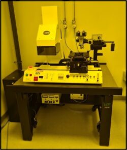
MicroWriter ML2 (Durham Magneto Optics Ltd), an innovative direct-write optical lithography system designed for rapid prototyping and small-volume manufacturing. Perfect for R&D laboratories and cleanrooms, the MicroWriter ML2 departs from traditional photolithography by eliminating the reliance on physical masks. Instead, it uses a software-based mask approach that delivers unmatched flexibility and efficiency. By projecting exposure patterns directly onto photoresist using computer-controlled optics, the system bypasses the time and expense associated with mask fabrication, making it ideal for environments requiring frequent design updates.
The MicroWriter ML2, featuring an active temperature stabilization system, maintains the internal temperature of the equipment and the exposed wafer within a 1°C range. It is equipped with ten 405 nm lasers: one with 0.6 µm resolution, one with 1 µm resolution, and eight with 5 µm resolution, making it suitable for exposing S1813 or equivalent photoresists. For SU-8 exposure, the OPT-UV module provides a 375 nm laser, offering resolutions from 1 µm to 5 µm.
The system supports wafers up to 230 mm (9") in diameter and can write across an area of 195 mm x 195 mm (7.7" x 7.7"). Additionally, it accommodates single wafer pieces as small as 1 mm².

The device includes three imaging cameras for precision and versatility:

  1. A red laser Scanning Laser Microscope (SLM) capable of detecting resist patterns with minimal intensity contrast.
  2. A 5x real-time video microscope with red-light illumination for rapid surface scanning.
  3. A 40x real-time video microscope with red-light illumination for detailed observation of sub-micron surface marks.

The MicroWriter ML2 is highly versatile and supports a wide range of advanced applications. In microelectronics and semiconductor devices, it facilitates the precise fabrication of integrated circuits and nano-scale components. For spintronics, it plays a crucial role in advancing spin-based electronic technologies. In MEMS and NEMS, the system supports the development of micro- and nano-electromechanical systems, including sensors and actuators. Furthermore, its capabilities extend to microfluidics and lab-on-a-chip applications, enabling the creation of miniature devices for biological and chemical analysis.
Packed with innovative features, the MicroWriter ML2 ensures high precision and functionality. Its Wafer Inspection Tool automates the quality assessment process by performing autofocus, visiting predefined coordinates, and capturing high-resolution microscope images. This allows efficient inspection of wafers with multiple dies. The Surface Profilometer Tool enhances fabrication accuracy by measuring Z-variations along the X- or Y-axis, ensuring optimal surface profiling.
The Automatic Marker Detection and Correction feature leverages primary and secondary alignment markers across the wafer to correct positional deviations, ensuring precise alignment between existing structures and new overlay exposures. With its Wide Field Viewer, the system can capture and stitch multiple images to create a seamless, large-area visualization of the wafer, aiding in comprehensive analysis. Additionally, the Virtual Mask Aligner mimics the traditional mask aligner experience, enabling simultaneous visualization of the virtual mask and wafer through a microscope for enhanced alignment precision.
The MicroWriter ML2 offers several significant advantages. Its software-controlled mask eliminates the need for physical mask fabrication, allowing for quicker design changes and cost savings. Advanced features like marker correction and surface profilometry deliver unparalleled precision, even for intricate designs. With its user-friendly interface and compact design, the system is accessible and adaptable, suitable for both small R&D labs and larger cleanroom environments.

Thermal Evaporation Coating System (Edwards Auto306)

Thermal Evaporation Coating System (Edwards Auto306)

The Edwards Auto306 Thermal Evaporation Coating System is a robust and versatile tool designed for thin-film deposition, widely used in both research and industrial applications. This system is particularly valued for its ability to create high-quality coatings on a variety of substrates, ensuring precision and reliability in the deposition process. It is a preferred choice for thin-film fabrication, especially in advanced materials science and nanotechnology, where consistent performance and ease of use are essential.
One of the key features of the Edwards Auto306 is its high-performance thermal evaporation capability, which uses thermal energy to vaporize materials. This process ensures the uniform deposition of thin films, providing excellent adhesion and high-quality coatings. The system is highly compatible with a wide range of materials, including metals, oxides, and other materials, making it adaptable to various applications in different fields. The system's precise thickness control is another standout feature, as it integrates monitoring systems that allow for accurate control over film thickness, ensuring reproducibility and consistency in results.
In addition to its high precision, the Edwards Auto306 is compact and user-friendly, designed to be easy to operate while occupying minimal space. This makes it ideal for use in research laboratories and small-scale production environments. It also guarantees vacuum integrity, maintaining ultra-high vacuum (UHV) conditions that ensure contamination-free deposition, which is critical for high-quality thin-film creation.
The system is built on advanced technology, incorporating a high-vacuum chamber and thermal evaporation sources that allow for precise and uniform film deposition. The Edwards Auto306 supports the use of multiple evaporation sources, which enables the sequential or co-deposition of materials. This feature is particularly useful for creating complex multi-layered structures, which are essential in many advanced applications.
The Edwards Auto306 has a wide range of applications across various industries. In microelectronics, it is used for the deposition of conductive and insulating layers necessary for integrated circuits and MEMS devices. In the field of optics, it is employed for fabricating anti-reflective coatings and optical filters. The system also plays a significant role in energy applications, such as the creation of thin-film solar cells and battery components. In material science, the Edwards Auto306 is used for developing protective coatings, sensors, and other advanced materials. Finally, in the field of nanotechnology, the system is used for depositing nanostructured materials for innovative devices.
In summary, the Edwards Auto306 Thermal Evaporation Coating System is a reliable and consistent tool for thin-film deposition, offering precise thickness control and adaptability to a wide range of materials. Its advanced features, combined with its versatility, make it an invaluable asset in the development of thin-film technologies across a variety of research and industrial applications.

MiniLab 080 (Moorfield Nanotechnology)

MiniLab 080 (Moorfield Nanotechnology)

The Moorfield MiniLab 080 is a high-performance, compact system designed for advanced thin-film deposition and nanotechnology applications. With its flexibility, precision, and efficiency, it is perfectly suited for use in research laboratories, universities, and industries aiming to achieve high-quality coatings on a variety of substrates. Its design ensures that users can conduct advanced experiments while maintaining a space-efficient laboratory setup.
One of the standout features of the MiniLab 080 is its flexible deposition options. It supports multiple deposition techniques, including thermal evaporation, electron beam evaporation, and magnetron sputtering, which allows for a broad range of material processing capabilities. This versatility makes it ideal for researchers and industries working with diverse materials and thin-film applications. Additionally, the system’s compact design makes it easy to integrate into smaller research labs or production environments, without sacrificing performance or capability.
The MiniLab 080 ensures high vacuum performance, providing ultra-high vacuum (UHV) conditions essential for producing thin films free from contamination. This feature is critical for the precision required in advanced thin-film deposition processes. The system also includes precise process control with integrated monitoring and real-time adjustment capabilities, allowing for reproducible results and fine-tuned deposition processes. This precision ensures consistent outcomes for high-quality thin films, making it ideal for research where accuracy and control are paramount.
Another key advantage of the MiniLab 080 is its substrate versatility. The system is compatible with substrates of various sizes and types, meeting the needs of a broad range of applications. Whether working with small-scale research samples or larger production runs, this flexibility allows users to achieve their desired results across diverse experimental and industrial demands.
The MiniLab 080 is engineered with advanced vacuum technology and robust deposition sources, ensuring uniform thin films with controlled thickness and composition. Its modular design allows for customization to meet specific experimental requirements, making it adaptable to a variety of research and production needs. This capability allows researchers to experiment with different materials, coatings, and technologies, all within a single, reliable system.
In terms of applications, the Moorfield MiniLab 080 excels in several cutting-edge fields. In nanotechnology, it is used to develop nanostructured films and devices for emerging applications. In microelectronics, it facilitates thin-film deposition for semiconductor devices, MEMS, and integrated circuits. The system is also valuable in optoelectronics, where it is used to create films for LEDs, photodetectors, and optical coatings. Additionally, it plays a significant role in energy applications, such as thin-film fabrication for solar cells, batteries, and supercapacitors. Finally, in material science, it is employed for research on advanced coatings, sensors, and protective films.
Overall, the Moorfield MiniLab 080 offers a compact, reliable, and customizable platform for thin-film deposition. Its wide range of deposition techniques, combined with precision engineering and advanced vacuum technology, makes it an essential tool for advancing research and innovation in nanotechnology and material science.

Additional Instruments

In addition to our advanced thin-film deposition and surface characterization tools, we provide a range of complementary instruments to support diverse research and industrial processes. These include high-performance ovens, precision measuring equipment, and vacuum systems designed to meet the rigorous demands of modern laboratories.

  • Ovens
    We offer a selection of high-quality ovens for heating, drying, and thermal processing:
    Philip Harris Ovens: Known for reliability and consistent temperature control, suitable for general lab use.
    Carbolite Ovens: High-performance ovens capable of reaching elevated temperatures, ideal for advanced material processing and annealing.
    Genlab Prime Ovens: Versatile and energy-efficient ovens designed for precision heating and drying applications.
  • Explorer Analytical Balance: A highly accurate and reliable balance for precise measurement of materials. Featuring advanced technology and a user-friendly interface, it is perfect for weighing samples with high precision, essential in analytical and material sciences.
  • SciSpin One50 Spin Coater: A high-precision spin coater for uniform deposition of thin films, photoresists, and coatings on substrates. Its advanced control system ensures consistency and repeatability, making it a vital tool for microfabrication and nanotechnology research.

Supporting Advanced Research
These instruments enhance the capabilities of our lab, providing the infrastructure needed to conduct comprehensive material analysis, sample preparation, and processing. Whether it’s heating, weighing, vacuum processing, or coating, our equipment ensures accuracy, efficiency, and reliability across a wide range of applications.